About Microelectronics
From a materialographic point of view, microelectronics can be divided into three types of samples:
- Silicon wafers
- Integrated Circuits (IC) and components
- Printed Circuit Boards (PCBs)

From a materialographic point of view, microelectronics can be divided into three types of samples:
Thin slices of the cylindrical silicon ingot are materialographically prepared for analysis by, typically, IR-microscopy, and FTIR- Spectroscopy.
Wafer fabrication includes many repeated processes to produce complete integrated electronic circuits on the wafer substrate surface and, subsequently, sectioning into individual wafer dice.
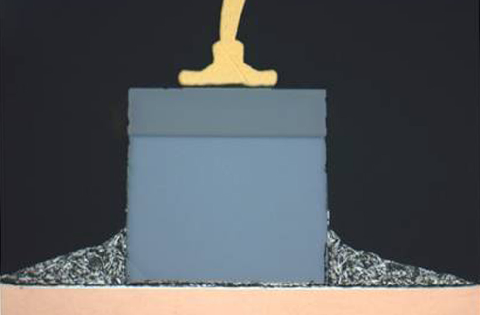
Inspection of tiny parallel or cross sections of the wafer in its non-encapsulated form is done after accurate materialographic polishing. Details in the integrated circuit are studied in a light or electron microscope, depending on the scale and the type of analysis.
Thin slices of the cylindrical silicon ingot are materialographically prepared for analysis by, typically, IR-microscopy, and FTIR- Spectroscopy.
Wafer fabrication includes many repeated processes to produce complete integrated electronic circuits on the wafer substrate surface and, subsequently, sectioning into individual wafer dice. Inspection of tiny parallel or cross sections of the wafer in its non-encapsulated form is done after accurate materialographic polishing. Details in the integrated circuit are studied in a light or electron microscope, depending on the scale and the type of analysis.

1. Miniature dimensions require specialized equipment and accessories suitable for handling small samples. The requirements to the accuracy in the materialographic processes, like cutting and grinding, are also more pronounced for samples defined by dimensions in the µm range.

2. Complex material compositions are common in microelectronics where soft metals, ceramics, and composites are often closely packed. This makes the choice of preparation methods and parameters a compromise, carefully selected to meet the specific requirements.

3. Controlled and accurate preparation is needed when small targets are the subjects for the examination. Solutions with high mechanical precision, optical measuring units, and mechanical stops are the modern automated or optimized solutions of the more basic grind-and-look technique.
Depending on what kind of sample needs to be investigated, the cutting can be done on various precision cutoff machines.
An electroplated diamond wheel for cutting plastics or a resin bonded diamond wheel is recommended.
In any case, the cut should be placed far enough from the actual area that is to be observed, to avoid possible direct damage to it. The remaining material can then be carefully ground away after sectioning. The more carefully this initial step is carried out, the less likely it is for cracks to be introduced in ceramic, chips, and glass, or cause delamination of layers or solder spots.
For extraction of PCB coupons, dedicated sampling equipment is brought into use. Automation and optical measurement techniques enable high precision drilling and routing of pinpointed coupons. For sensitive or small samples, it is advisable to impregnate the sample before cutting.
Cold mounting resins, with low curing temperatures, are recommended to avoid the influence of heat on solders and polymers. For small or brittle samples, e.g. silicon wafers, a low shrinkage resin is preferred in order to minimize the risk of cracks.
Mounting methods differ depending on the analytical method used.
For dedicated systems, components may be mounted directly in the special sample support used for via inspection or target preparation, for example.
For manual and semiautomatic grinding and polishing of microelectronics, conventional equipment can be used. Aligning the sample and controlling the material removal is secured by special sample holders as a more accurate alternative to the manual grind-and-look method.
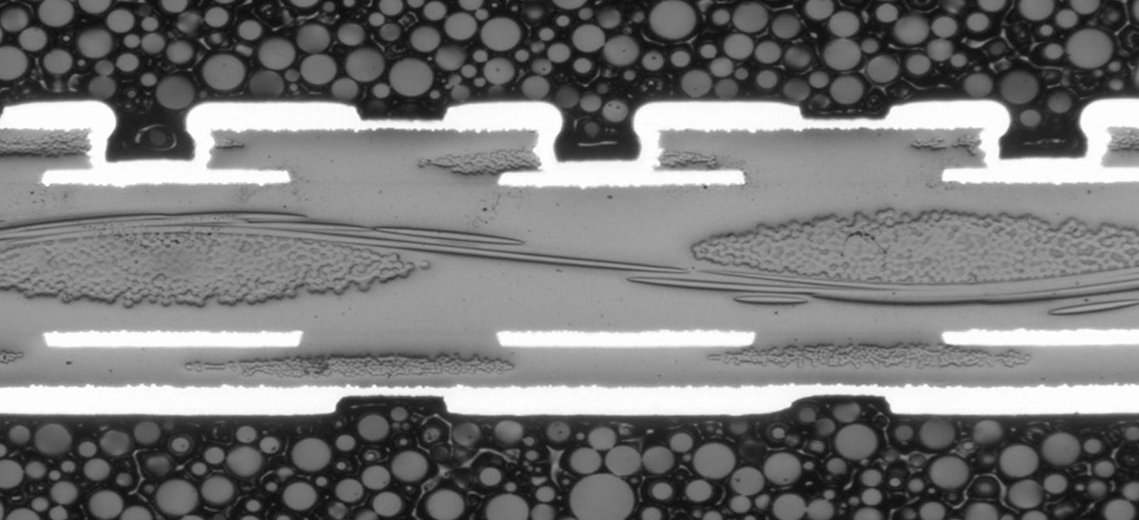
Parallel and cross sections of thin and brittle silicon wafers, arrays of solder balls of lead or tin, PCBs with copper-plated vias on brittle ceramic or ductile polymeric substrate, and cross sections of ICs with silicon, ceramic, gold, copper, aluminum and tin within a few hundred microns are examples of material combinations to consider, in the choice of grinding and polishing methods.
Requirements for removal rate, planeness, relief, edge retention, and smearing often determine the choice of grinding and polishing surfaces and suspensions. Around 25 dedicated methods are found in the e-Metalog for electronic components, covering a broad selection of materials combinations and preparation requirements.